Electric Fence energiser development
By Eyobed on 3/14/2025
Microcontroller Based Electric Fence Energizer: A Technical Implementation
This project documents the design and prototyping of a non-lethal electric fence energizer built as part of an electronic engineering degree program at Addis Ababa University's Faculty of Technology.
The design emerged from studying existing commercial solutions and reverse-engineering their core principles, then reimagining the implementation with modern microcontroller based approach.
System Architecture
The energizer combines a high-voltage pulse generator with some monitoring and control capabilities. The system manages power delivery through a fault tolerant supply with battery backup, while simultaneously monitoring fence integrity through breach detection and wire tension sensing.
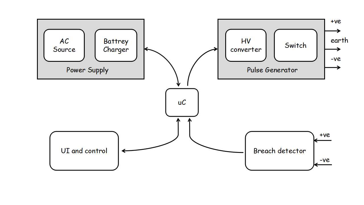
Microcontroller Foundation
The Microcontoller used in the project is Atmega32u4. It controls the high voltage pulse generator, monitors the fence integrity, and provides a user interface for the user to control the energizer.
Beyond the core functionality, the microcontroller enables extensions like alarm triggering, remote control integration, and access control interfacing that would be difficult or impossible with traditional analog designs.
High Voltage Generation
Converting a low-voltage source like a 9V or 12V battery into the kilovolt-range pulses required for effective deterrence presents several design challenges. After evaluating multiple topologies, I selected a pulse transformer approach for its simplicity and reliability in similar applications.
The implementation had two stages: a high voltage converter that charges a reservoir capacitor to approximately 360V, and a discharge circuit that dumps this stored energy through a pulse transformer at one second intervals to generate the fence output.
High-Voltage Converter Design
This circuit converts 12 V DC from the system supply rail to 360 V DC in order to charge a reservoir capacitor. The converter must deliver enough power to recharge the capacitor between discharges occurring once per second, while avoiding excessive output power that could unintentionally keep the TRIAC conducting.
Due to the requirement for galvanic isolation and the benefit of a simple control structure, a flyback converter topology is selected.

1. Design Requirements
Energy and Power
The capacitor discharges an energy of:
E = 3 J
once every second. Therefore, the required output power is:
P_out = E / t P_out = 3 J / 1 s = 3 W
Assuming an efficiency of 80%:
P_in = P_out / 0.8 P_in = 3 / 0.8 = 3.75 W
Electrical Specifications
- Input voltage: V_in = 12 V
- Output voltage: V_out = 360 V
- Switching frequency: f_s ≈ 70 kHz
2. Maximum Duty Cycle
The conversion ratio of a flyback converter is similar to that of a buck boost converter. The reflected output voltage on the primary side is:
V_RO = (D / (1 − D)) × V_in
Choosing a duty cycle of:
D = 0.5
This makes the output voltage primarily dependent on the transformer turns ratio.
The total voltage stress across the transistor collector emitter terminals is:
V_CE = V_in + V_RO
Substituting values:
V_CE = 12 V + 12 V = 24 V
3. Transformer Primary Inductance (L_M)
The minimum primary inductance is calculated for worst-case conditions (full load and minimum input voltage):
L_M = (V_in × D)² / (2 × P_in × f_s)
Substituting values:
L_M = (12 × 0.5)² / (2 × 3.75 × 70,000) L_M ≈ 68 µH
4. Peak Collector Current
The average input current is:
I_DC = P_in / (V_in × D)
I_DC = 3.75 / (12 × 0.5) I_DC = 0.6 A
The peak-to-peak current ripple is:
ΔI = (V_in × D) / (L_M × f_s)
ΔI = (12 × 0.5) / (68 µH × 70 kHz) ΔI ≈ 1.26 A
The peak collector current is:
I_peak = I_DC + (ΔI / 2)
I_peak = 0.6 + 0.63 I_peak ≈ 1.23 A
Based on collector–emitter voltage, peak collector current, and input power, a suitable transistor is selected. The 2SD882 transistor is used; according to the manufacturer datasheet, it is rated for:
- Collector–emitter voltage: 30 V
- Collector current: 3 A
- Power dissipation: 12.5 W
These ratings provide sufficient margin for the converter.
5. Transformer Core Selection and Primary Turns
Based on core manufacturer (TDK) selection data, an EE16 core is chosen with a cross-sectional area:
A_e = 19 mm²
The minimum number of primary turns is calculated as:
N_P(min) = (L_M × I_peak) / (B_sat × A_e) × 10⁶
Substituting values:
N_P(min) = (68 µH × 1.23 A × 10⁶) / (0.35 × 19)
N_P(min) ≈ 12.5 turns
Therefore, the primary winding is selected as:
N_P = 12 turns
6. Secondary Winding Turns
The turns ratio is calculated from the reflected voltage:
Turns ratio = V_RO / V_out Turns ratio = 12 V / 360 V = 1 : 30
With 12 primary turns, the required secondary turns are:
N_S = 12 × 30 = 360 turns
7. Oscillator Implementation
First Prototype
The PWM signal is generated using the UC3842 current-mode PWM controller. Although designed for MOSFET drive, it can also be used with BJTs by employing base current-limiting resistors.
The oscillation frequency is set by an RC network:
f = 1.72 / (R × C), where R > 5 kΩ
For R = 10 kΩ and a target frequency of 50 kHz:
C = 1.72 / (10,000 × 50,000) C ≈ 3.44 nF
A standard capacitor value of 3.3 nF is selected.
Second Prototype
The UC3842 requires a startup voltage of approximately 16 V, which exceeds the available supply voltage. To overcome this limitation and reduce cost, a self-oscillating ringing choke flyback converter is implemented instead.

Although this topology uses fewer components, its operation is more complex than PWM controller based designs. A feedback winding is used to derive the switching signal directly from the transformer output, enabling self-oscillating operation.
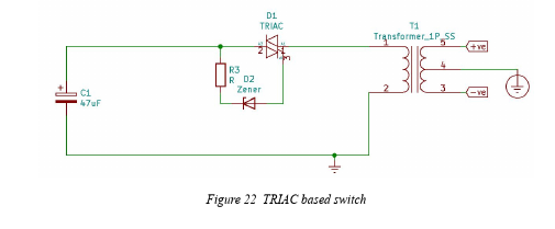
The discharge circuit
This section must produce 7.2kV bipolar pulses with pulse widths under 50ms and energy content below 3 joules to remain within non lethal specifications. A center-tapped pulse transformer handles the voltage multiplication while enabling bipolar operation.
The switching element that triggers each discharge can be implemented several ways, but a TRIAC offers good advantages for this application. TRIACs handle large instantaneous currents without degradation, provide reliability, and naturally turn off when current drops below their holding threshold. This last characteristic is particularly useful since it prevents the device from latching on during the capacitor discharge cycle.
Methodology
Building and validating the circuit required juggling multiple simulation tools, each chosen for its particular strengths. SimulIDE handled the digital control logic with near real time simulation speeds that made rapid iteration practical, though its analog capabilities are limited. For the power electronics, LTspice provided high fidelity analog simulation with an extensive component library, though it cannot simulate digital circuits. Proteus VSM can handle mixed analog-digital simulation but proved too slow for iterative development work in its demonstration version, so I relegated it to final verification of integrated subsystems.
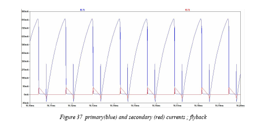
Measured Performance
The flyback converter operates as a ringing choke converter (RCC) configuration, which shows up in the waveforms as a duty cycle that adapts based on load conditions. Under no load conditions, the duty cycle drops well below 50%, which is characteristic behavior for this topology. The primary and secondary inductor currents show the expected relationship given the turns ratio, with secondary currents proportionally reduced due to the step-up transformation.
The fence output waveforms from the LTspice simulations confirm that the pulse transformer and discharge circuit achieve the specified voltage and timing parameters. The bipolar pulse shape results from the center-tapped transformer configuration, with each half-cycle drawing from opposite sides of the secondary winding.
Physical Implementation and Prototyping
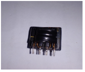
Transformer Fabrication
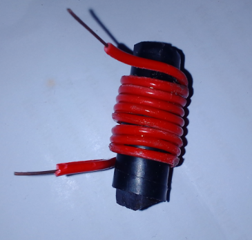
Both transformers in the energizer required custom winding due to the specific voltage ratios and power handling requirements. The flyback transformer originally targeted an EE16 ferrite core, but I switched to a larger core during fabrication to provide margin for winding imperfections that might otherwise prevent the bobbin from closing properly. Each winding layer : primary, secondary, and auxiliary received electrical tape insulation between them to ensure adequate voltage standoff and prevent interwinding breakdown.
The pulse transformer presented a more demanding insulation challenges. Operating at several kilovolts, these transformers will arc internally if the insulation scheme fails, as documented extensively in highvoltage transformer construction guides. I wound the primary using thick plastic-insulated wire on a ferrite rod core, while the secondary used enamel-coated magnet wire. To prevent voltage breakdown through the secondary winding, I added extra insulation layers every 20 turns. This technique distributes the voltage gradient more evenly along the winding length and prevents the electric field concentration that causes internal arcing.
Iterative Hardware Development
The physical prototyping followed a staged approach that balanced development speed against permanent assembly. Each circuit subsystem started on a breadboard for initial verification and troubleshooting. Once a subsystem demonstrated correct operation and met its specifications, I transferred it to a perforated prototyping board for permanent assembly.
The flyback converter serves as a representative example of this workflow. After simulating the circuit and selecting component values, I built the converter on breadboard with the handwound transformer. This revealed issues that simulation missed, such as parasitic oscillations from long breadboard leads and the sensitivity of the RCC topology to component placement. After resolving these issues and confirming proper operation with oscilloscope measurements, the circuit moved to perforated board.

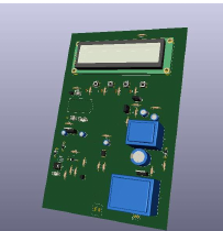
The complete assembly occupies a perforated board measuring 6.5cm by 14.5cm. It includes the flyback converter, discharge circuit with TRIAC switching, microcontroller interface circuitry, and the necessary current sensing and protection elements. The compact layout required attention to high voltage spacing and component orientation to prevent arcing between circuit nodes at different potentials.
PCB Development
Moving beyond the prototype stage, I designed a preliminary PCB using KiCad EDA software. The PCB layout addresses several issues that are difficult to manage on perforated board, particularly proper ground plane implementation, controlled impedance for switching nodes, and creepage distances for high voltage sections.
Practical Considerations
One subtle but important design point concerns the interaction between the flyback converter's output power and the TRIAC's holding current. If the converter supplies too much current during the discharge phase, the TRIAC may remain latched even after the capacitor voltage drops, effectively creating a short circuit across the high-voltage rail. Careful component selection and converter design ensures the discharge current falls below the TRIAC's holding threshold before the converter can sustain conduction, allowing proper circuit reset between pulses.
The microcontroller integration opens possibilities beyond simple pulse generation. Monitoring fence voltage and current during normal operation can detect wire breaks or short circuits. Tracking discharge timing and energy delivery enables diagnostic logging and maintenance alerts. Remote control capabilities allow the fence to be disabled safely during maintenance or integrated with broader security systems. These features transform a relatively simple pulsed power supply into an intelligent perimeter security device.